Mathworks released the RF PCB Toolbox with the latest release of MATLAB, R2021B, this toolbox allows the creation and visualisation of “Transmission lines, Couplers, Splitters, Filters, and More”, this was something that I wanted to a go at particularly the design of the filters. These filters that are just made of PCB traces have always fascinated me and given the tools that should allow me to design them, I decided to give it a go. I’ve always though of RF design as a bit of a dark art, and as someone who spends a lot of time around Software Defined Radios in my day job, I find the more I know the less I truly understand, so being able to create some filters with just a few lines of code seemed like a great idea.
The filter I decided to have a go at is one to work in the 2.4GHz ISM band, centred at 2440MHz, with a pass band of 80MHz, then as much stop band attenuation as possible. After having a look though the documentation I decided to have a go at the Hairpin filter.
From the examples in the documentation for the toolbox which walk you though building the filter, I built myself a script with all the user configurable user configurable variables at the start. We begin by defining these parameters that we are going to use in our filter implementation, this includes variables such as our filter order n and then specific properties such as the substrate and conductor that will make up our filter. In my case here as i’m looking to build the filter on a standard standard PCB, we are setting these variables based on there spec sheet, for FR4 and copper rather then more expensive options they default to.
N = 3;
Ripple = 0.1;
BandWidth = 10;
Z0 = 50;
f = linspace(1500e6,3000e6,601);
EpsilonR = 4.5;
Height = 1.6e-3;
d = dielectric("FR4");
d.EpsilonR = EpsilonR;
m = metal("Copper");
With all these high level variables defined, I can then look to start building up my filter object with them, and then calling the filter design function. The filter design will generate a filter that matches my design requirements, and output it to the filter object.
filter = filterHairpin();
filter.FilterOrder = N;
filter.Substrate = d;
filter.Conductor = m;
filter.Height = Height;
filter = design(filter,2440e6,'FBW',BandWidth,'RippleFactor',Ripple);
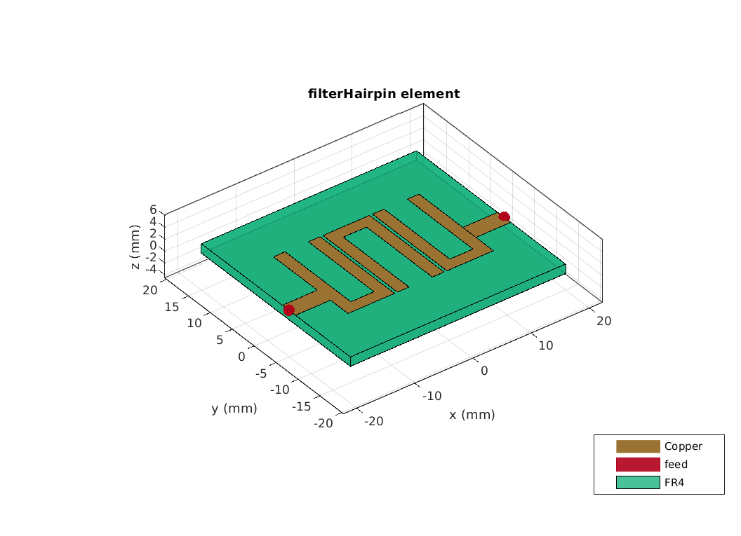
With this filter object we can now start to explore the filter design that has been created, in my case the first thing I wanted to see was what the filter actually looked like, to do this you just simply use the show(filter); command, which generates a plot with a 3D visulisation of the filter which has been designed, as shown bellow.
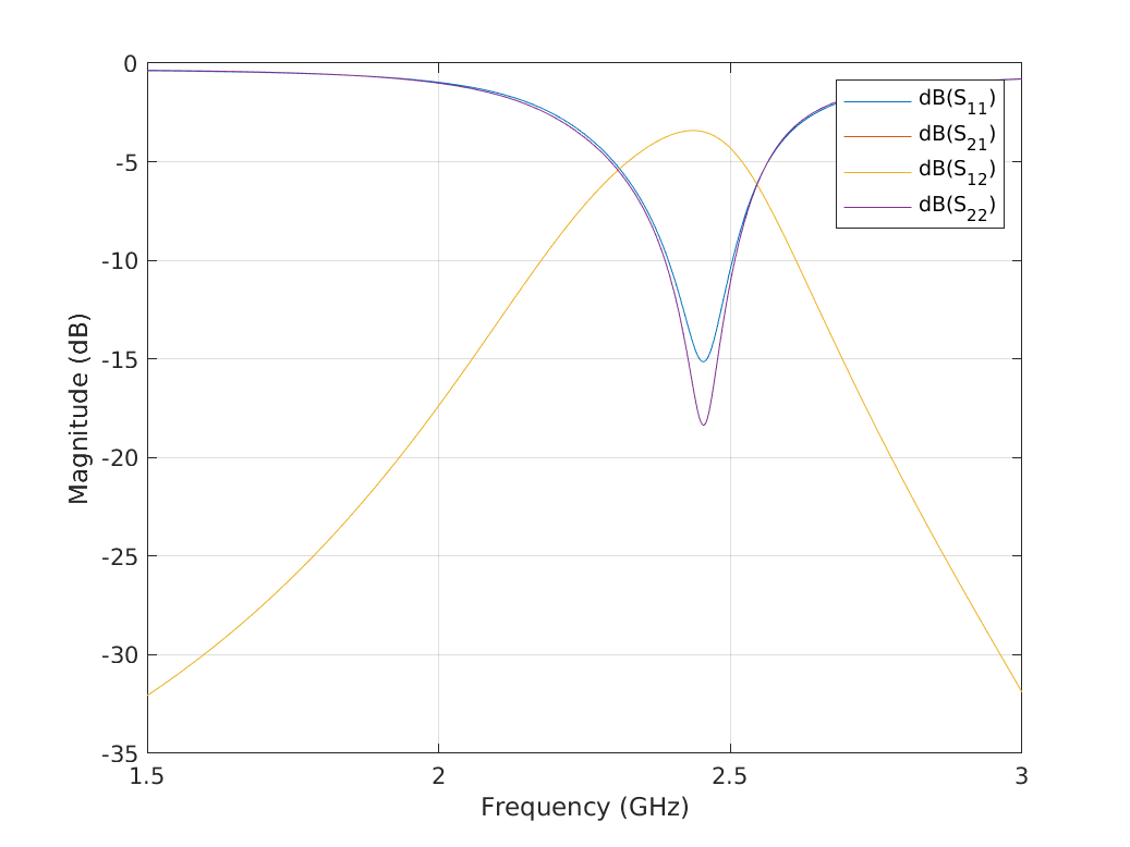
The next big question is how well is this filter actually going to work, for that I wanted to look at the gain of the filter at different frequencies, for this we need to generate the s-parameters for this design, and the plot the result.
spar = sparameters(filter,f);
figure()
rfplot(spar);
This command take a while to run, as I have set this up with it running are 601 different frequency points to produce a high resolution plot, with the test points stored in the variable f, but this helps to produce a graph which is shown bellow with our simulated performance.
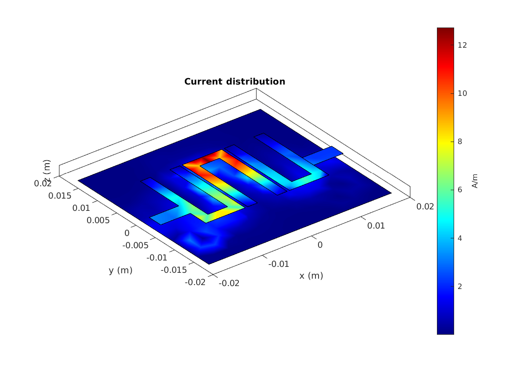
The next plot is the Current Distribution, i’m not really sure how you interpret this plot, but it does look cool, and one day I might look back at this post and actually undersatnd what it is actually telling me.
With this 3rd order Hairpin filter designed in MATLAB, the next stage is where you export it, they way of doing this which is given in the documentation is to export to gerbers. this seemed like a great option at first look but I soon came up with some issues with it, the first is this is designed to generate Gerber files and send them straight of for manufacture, and thats not what I wanted to do, the second issue I found was I couldn’t find a way to export the filter design in a way that I could import it into KiCAD as a component footprint I could use on a PCB design.
My way round this was to export the gerbers, and then import the Gerbers into kiCAD and edit them there in PCBNew, to export the filter it is just the case of running a couple of simple lines of code in MATLAB
p = pcbComponent(filter);
W = PCBServices.PCBWayWriter;
W.Filename = 'Filter_2440MHz_3';
C1 = PCBConnectors.SMAEdge_Samtec;
C2 = PCBConnectors.SMAEdge_Samtec;


C1.EdgeLocation = 'west';
C1.ExtendBoardProfile = false;
C2.EdgeLocation = 'east';
C2.ExtendBoardProfile = false;

[A,g] = gerberWrite(p,W,{C1,C2})
It actually took me a long time to work out how to add the connectors, and I’m not sure if it the correct way of adding the SMA connectors, but as I wanted an SMA on each side of the board this seemed the only way I could work out how to add them. The N-Type connectors worked as expected but I generally work with SMA at home. I had to disable the ExtendBoardProfile as this kept producing boards with area’s of the PCB Filter missing with the connectors floating away from the PCB in the resulting Plots and gerber files. I had to add in a port line length to and from the filter with filter.PortLineLength = 0.006; to force the designed filter to put the connectors where i wanted and stop MATLAB from placing the SMA’s ground connection within the filter. The issues like this all seemed to be a bit buggy, typical early release problems, but given this is the first release they will hopefully improve with time.
With the output files generated I then opened loaded the Gerber files into KiCad’s Gerber Viewer and imported the layer into PcbNew, this allowed me to add my own custom description text and logos onto the board, getting it ready to be sent of to be manufactured. one problem I did find at this stage, is that some random copper blocks appeared over the SMA connectors, which I removed, which I don’t think should have been added.
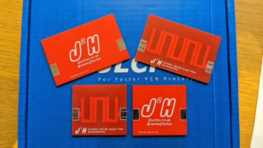
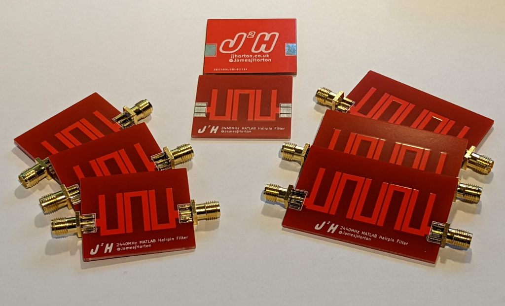
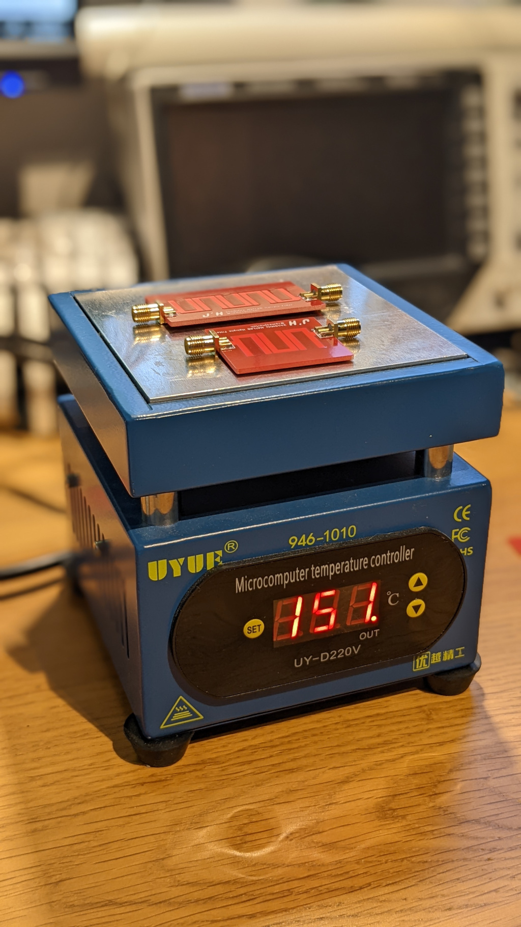
With all that sorted, I added my designs to my filters GitHub repo and ordered the PCB using the Gerber files that were generated by KiCAD. Once the PCB’s had arrived from JLCPCB about a month after I had ordered, it was time to add some SMA connectors and give them a test.
I’m using a NanoVNA to test them out, while not as good as a proper Network Analyser, but given the Nano VNA cost £60 it provides a great way of being able to get a good idea of there performance of these little filters at home.
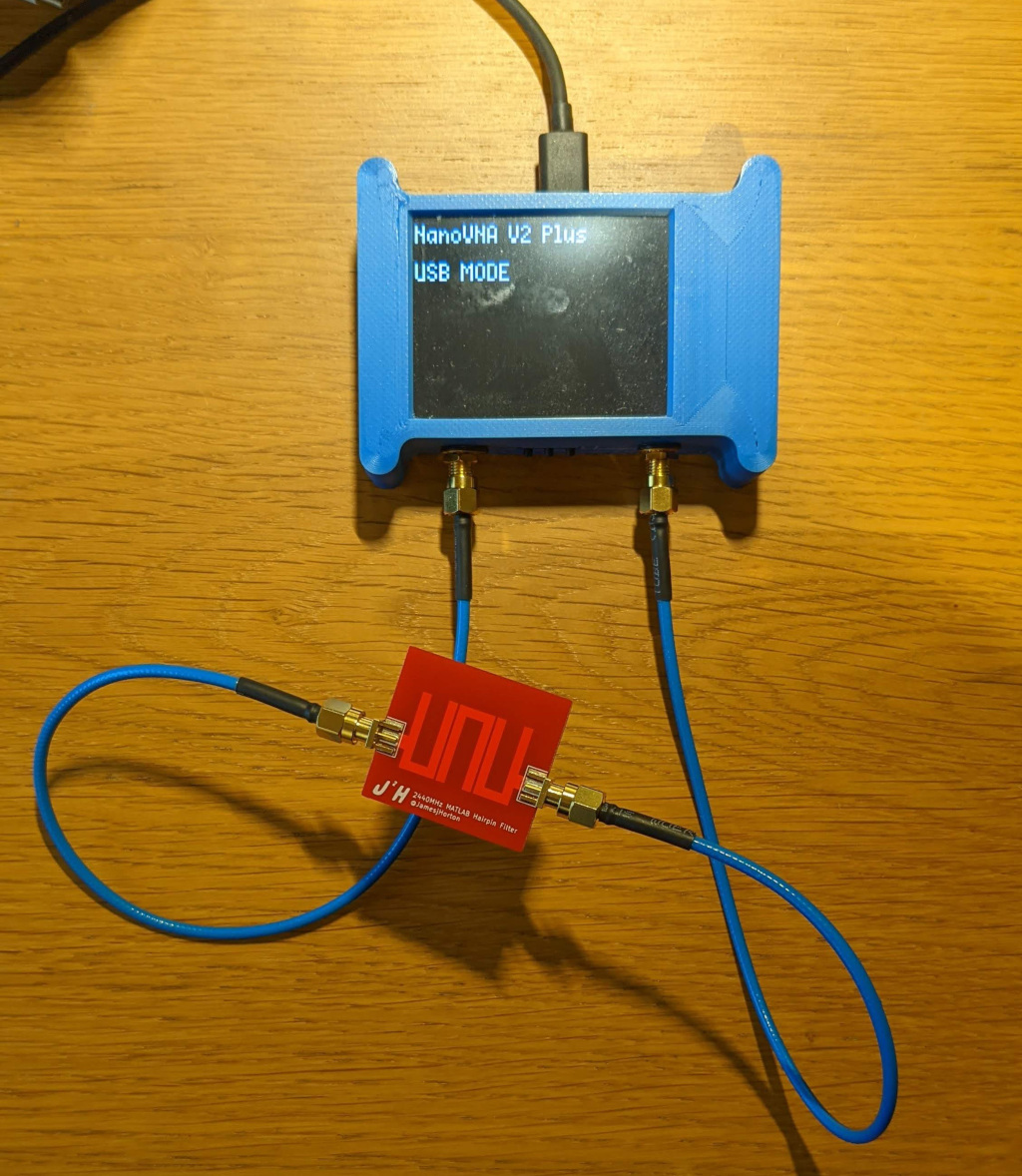
The NanoVNA can be used with PC based software, such as i’m using bellow, which is much easier to interact with rather than the tiny screen, though this interface I can also calibrate the results, and use the s-parameter menu, to take measurements of each of the filters, which can be stored to S-parameter files that can be imported into MATLAB for analysis.
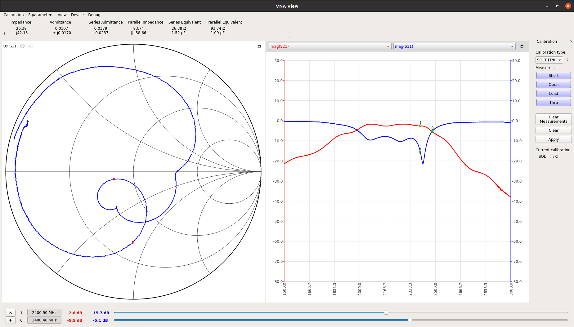
The main test here is if the filters that I have make actually match the simulation, so the best way to assses them is to compare the filter gain from 3 of the real thing and the Matlab Simulation to see if they match, and well there is a bit of a difference, as we can see bellow for the 3rd order filter.
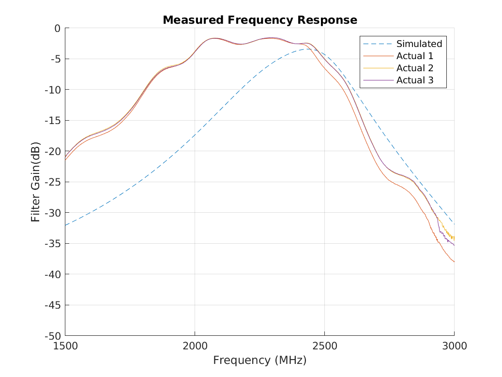
The 3rd order filter is almost close to what is expected, but with the pass band pushed to a lower frequency, and a wider pass band, the attenuation of the filter at frequencies above the designed pass band is actually similar to what is expected. With it producing a similar ammount of attenuation, with a similar roll of to the simulation.
We can also look at the results for the 5th Order Filter, which also shows a lot of similar characteristics, with the roll of at both high and low frequencies appearing to match the simulation, with the exception of the pass band being shifted to lower frequencies.
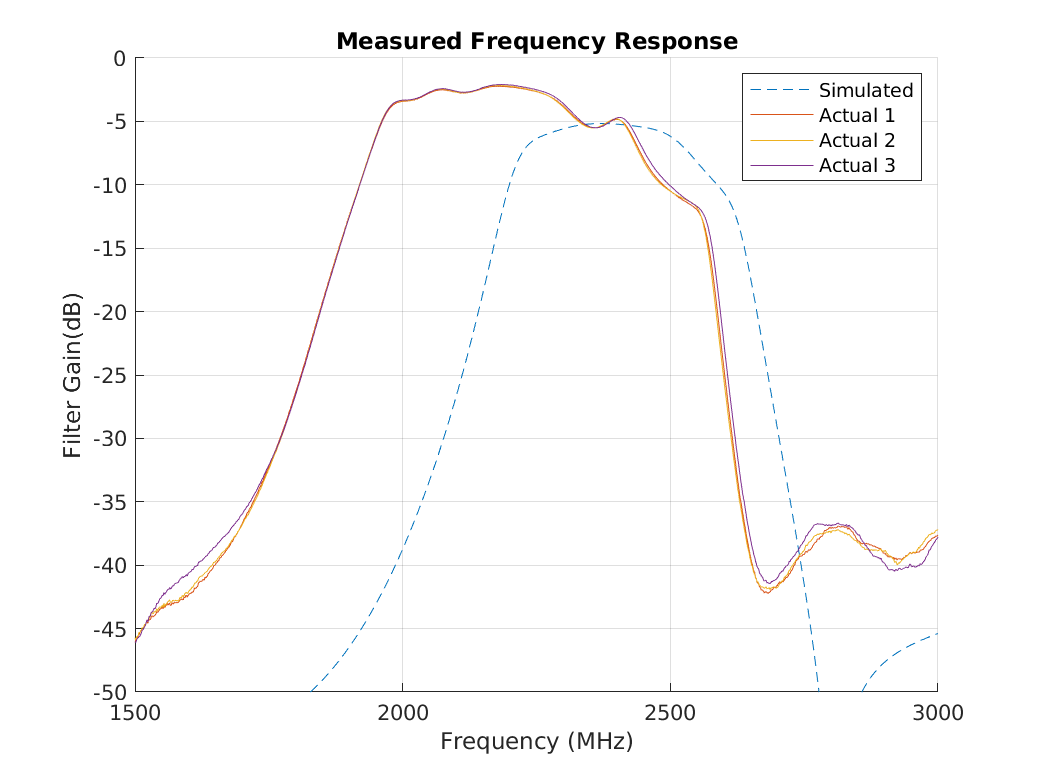
The fact the the results are both consistent between each of the types of filter and example of the filters produces similar results, make me think the is a systematic problem here. I think the issue point to there being a design error, and there are a couple of possible causes, the first of which is the PCB manufacturing. The PCB’s are low cost models costing just $2, and at that price accuracy is limited and this comes in more forms than one. The first is in terms of the accuracy of the PCB traces themselves, and then of the material used in the PCB’s themselves. One key parameter used in the PCB manufacture and filter design, this is the dielectric constant, which JLCPCB gives as 4.5 for a double sided PCB, which is typically a useful number to use but unfortunately this value actually varies with frequency which makes it more challenging to pick what to use when just working with standard FR4, this is not a problem if you are using a higher quality material, but when working on a budget there are limitations.
The next stage is experiment with simulating the filters that were originally created, and to see if by changing the dielectric constant I can match up the simulation with the measured results. this would mean that I could have a go at re-creating the filters with a corrected value for dielectric constant at 2.45GHz, when having a second attempt at building some filters.